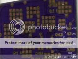

This is a photo etching procedure but it doesn't involve the use of photo lacquer. It uses dry photo resist films. Films are laminated onto the PCB boards and later exposed to UV light source.
There is also a UV exposing box with vacuum to press the artwork onto the PCB. This results in improved resolution and PCB quality. Vacuum is made with fish tank pump. After developing a basic circuit board, another two films are applied and UV-exposed with soldermask and stopmask layers. What really caught my attention is the process of making solder paste stencils. It is made in the same way as the PCB but the good thing is that the material is a very thin sheet of aluminium taken from a beer can. Excellent idea and a perfect material for this use!
view more...
Share


0 comments:
Post a Comment
Strictly Load Comments that contain elements of racial intolerance, provocation, and that notwithstanding Pornoaction Other. Putting is also prohibited Links Overstated In Comments Box. Give Feedback Related Content Post.